
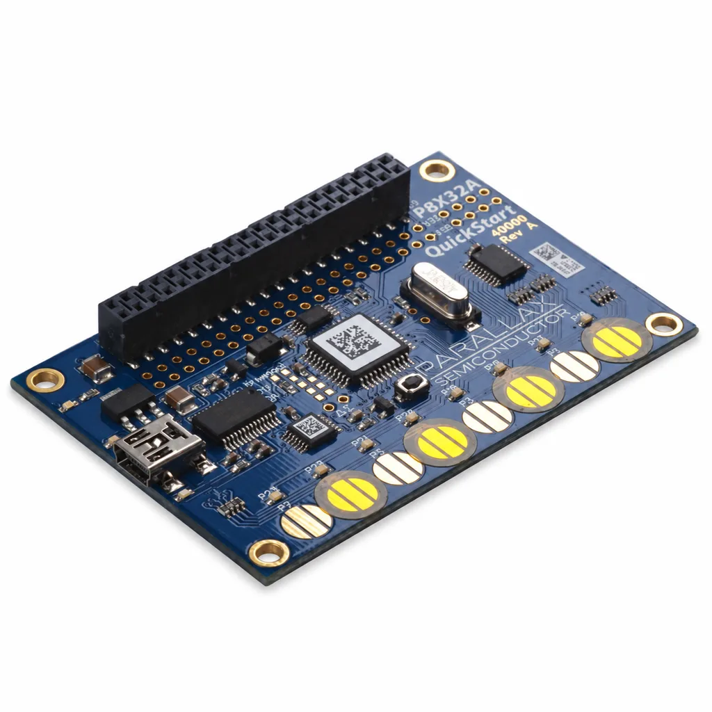
CL-8711 White Anti-Static Polyimide Label for Wave and Reflow Soldering
CL-8711 is a white glossy anti-static label built on a 1 mil (approx. 25 μm) polyimide (PI) film base, with a rated temperature range of -40 to 300 °C. According to the approved technical data, it can be used in wave soldering and reflow soldering processes, resists chemical reagents, and is halogen-free. Its anti-static value (surface resistance of at least 10^(8) Ω and at most 10^(11) Ω) and peel voltage below 100 volts help protect electrostatic discharge (ESD) sensitive components while the label is in use. The material is mainly applied in the electronics industry, commonly for process control and product traceability of printed circuit boards (PCBs) and sensitive components. Key selection conditions: confirm your peak process temperature and dwell time, your required ESD control level, expected chemical exposure, and your printing method before ordering.
- -40 to 300 °CRated temperature range
- ≥10^(8) Ω, ≤10^(11) ΩAnti-static value (surface resistance)
- <100 voltsPeel voltage
Product Overview
CL-8711 is an anti-static label material for electronics manufacturing: a white glossy coated label on a polyimide (PI) film base, 1 mil (approximately 25 μm) thick. PI is the film family generally chosen when labels must survive soldering-level heat rather than general-purpose room-temperature labeling. The technical data for this material places its main application in the electronics industry, where it is commonly used for process control and product traceability of printed circuit boards (PCBs) and sensitive electronic components.
The primary selection basis is thermal capability. The material is rated for a temperature range of -40 to 300 °C, and the technical data states that it can be used in wave soldering and reflow soldering processing, which usually exceed what general-purpose label materials can withstand. The data does not define a maximum exposure time or heating ramp, so match the rating against your measured soldering profile (peak temperature and dwell time) instead of assuming unlimited residence at the maximum temperature.
The second selection basis is electrostatic discharge (ESD) control. The anti-static value is specified as surface resistance of at least 10^(8) Ω and at most 10^(11) Ω, a range generally classified as static dissipative, which limits charge accumulation on the label itself. Peel voltage is specified as below 100 volts, restricting the charge generated when the release liner is removed during application. Together with the white glossy print surface for readable identification, these properties support labeling of ESD-sensitive components during process control and traceability, as stated in the technical data.
Limitations to verify before ordering: the technical data does not state label dimensions, roll or sheet packaging format, adhesive type, or printing-method compatibility, so confirm these against your printer and application process. Chemical reagent resistance and halogen-free status are stated without specific test conditions. The SGS/RoHS entry comes from the external source data for this material and is not presented as our own test report; verify the certification evidence your quality process requires. The temperature rating is a range statement, not a claim of long-term continuous exposure at the maximum temperature.
Core Advantages
High temperature resistance with anti-static behavior
The technical data lists the label as high-temperature resistant and anti-static: the PI (polyimide) base is rated for -40 to 300 °C, and the anti-static value is specified as surface resistance between 10^(8) and 10^(11) Ω.
Usable in wave and reflow soldering
The technical data states that the label can be used in wave soldering and reflow soldering processing, the soldering heat stages of electronics production lines.
Chemical reagent resistance, halogen-free
The technical data lists resistance to chemical reagents and a halogen-free composition, which matters where boards contact fluxes and cleaning agents during soldering and post-solder cleaning.
Protects ESD-sensitive components during label use
The technical data states that the label effectively protects sensitive components from electrostatic discharge (ESD) influence during label use, supported by a peel voltage below 100 volts at application.
Technical Specifications
| Coating | White glossy |
|---|---|
| Thickness | 1mil |
| Base material | PI |
| Temperature range | -40-300℃ |
| Anti-static value (surface resistance) | ≥10^(8)Ω,≤10^(11)Ω |
| Peel voltage | <100 volts |
| Certification standard | SGS/RoHS |
Typical Applications
Electronics industry
The technical data lists the electronics industry as the main application field for this label material.
PCB process control
Commonly used for process control of printed circuit boards (PCBs) and sensitive components; in these stages the label is exposed to soldering-level heat and chemical contact.
Product traceability of boards and sensitive components
Used for product traceability in electronics production: the white glossy surface carries identification that supports tracking boards and sensitive components through the process.
ESD-sensitive component identification
The anti-static value and low peel voltage support labeling near electrostatic discharge (ESD) sensitive components, where the technical data states the label helps protect components from ESD influence during use.
Frequently Asked Questions
What temperature range can the CL-8711 label withstand, and can it go through wave and reflow soldering?
The rated temperature range is -40 to 300 °C, and the technical data states that the label can be used in wave soldering and reflow soldering processing. The data does not specify a maximum dwell time or heating ramp, so compare the rating with your measured soldering profile, including peak temperature and time above each threshold, before committing the label to your process.
What does the anti-static value of at least 10^(8) Ω and at most 10^(11) Ω mean for protecting ESD-sensitive parts?
The anti-static value is specified as a surface resistance of at least 10^(8) Ω and at most 10^(11) Ω. In general ESD control practice this range is classified as static dissipative: the surface is neither highly insulating nor conductive, so it limits charge build-up rather than generating or holding high voltages. The technical data states that the label effectively protects sensitive components from electrostatic discharge (ESD) influence during label use.
What does a peel voltage below 100 volts mean when applying the label?
Peel voltage refers to the electrostatic potential associated with peeling the label from its release liner. The technical data specifies peel voltage below 100 volts; voltage is an electrical potential, not a quantity of charge. While peeling and applying labels near ESD-sensitive components, continue to follow your normal ESD handling procedures in controlled areas.
When should I choose this 1 mil PI label instead of a PET label?
This label uses a polyimide (PI) film base, 1 mil (approximately 25 μm) thick, rated for -40 to 300 °C. As general industry guidance rather than a claim about any specific product, PET label materials are usually selected where process temperatures stay comparatively low because they cost less, while PI materials are the usual choice when labels must survive soldering-level heat. Base the decision on your measured peak temperature and exposure time, not on the material name alone.
Is the label halogen-free, and what certification is listed?
The technical data lists the label as halogen-free and resistant to chemical reagents, and lists SGS/RoHS as the certification standard. These entries come from the external source data for this material and are not presented as our own test reports; verify the certification and test evidence your quality process requires before ordering.
Explore

Acid and Alkali Resistant Label
Chemical-resistant label construction for acid baths, paint-stripping solutions, alkali…
View details
Aluminum Foil High-Temperature Label
Coated aluminum label for metal processing, heat treatment and high-temperature part…
View details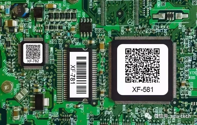
Anti-Static High-Temperature Polyimide Label
Anti-static polyimide label for ESD-sensitive electronics assembly and high-temperature…
View detailsNot sure which grade fits your printer and label?
Tell us the label material, printer model, environment and expected durability. We will recommend the right option.
