
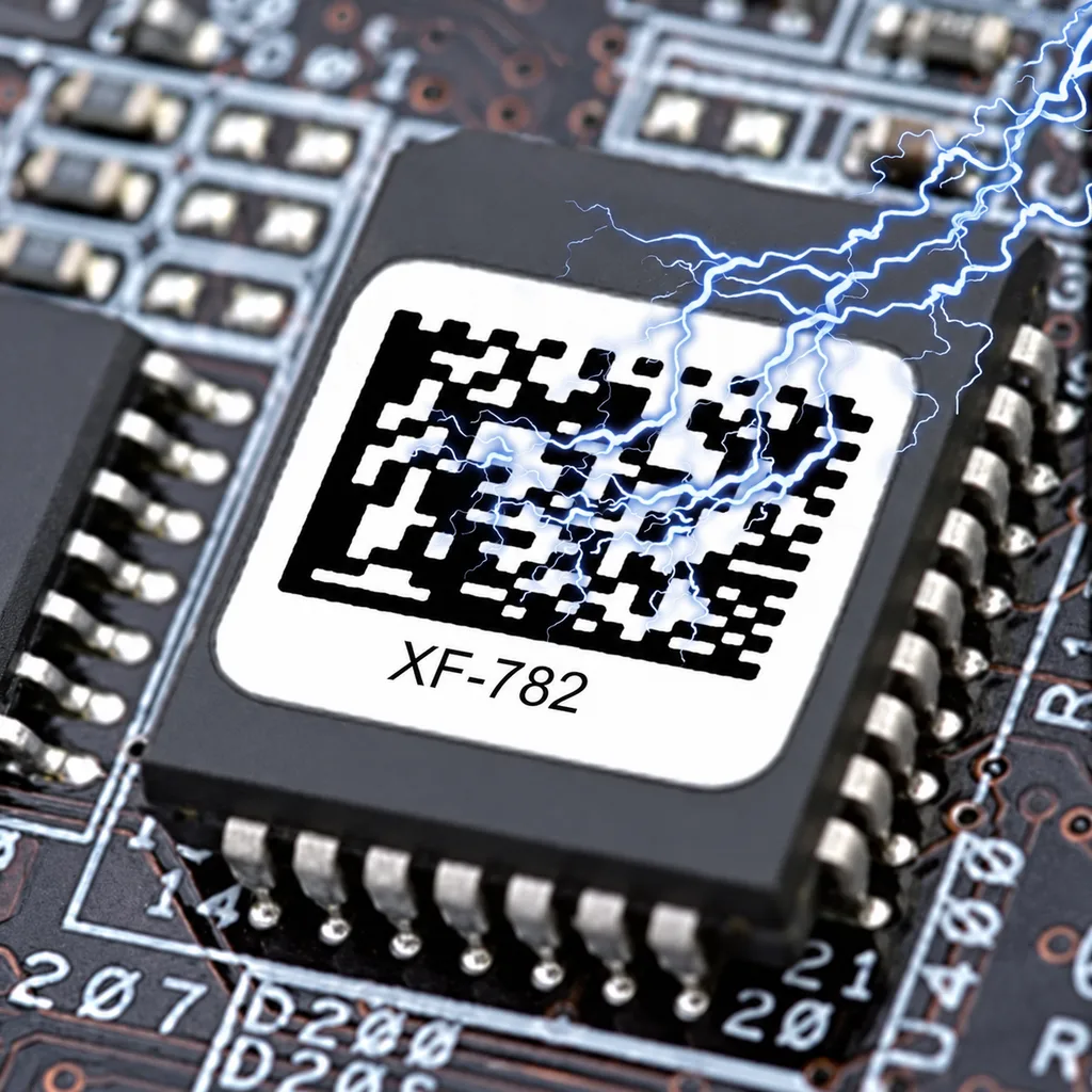
Antistatic Polyimide Labels for PCB Process Tracking — CL-782
CL-782 is a white gloss polyimide (PI) label material for printed circuit board (PCB) and sensitive-component process control and product traceability in electronics manufacturing. It is described for wave soldering and reflow soldering applications, with a listed temperature range of -40-300℃, an antistatic value of ≥10^(8)Ω and ≤10^(11)Ω, and a peel voltage below 100 volts. Selection should account for the actual thermal cycle and chemical exposure; the supplied information does not specify exposure durations or chemical test conditions.
- 2milThickness
- ≥10^(8)Ω,≤10^(11)ΩAntistatic value
- <100 voltsPeel voltage
Product Overview
This label material is intended for identifying printed circuit boards and sensitive components during electronics production. Its stated applications cover process control and product traceability, including wave soldering and reflow soldering. The construction information identifies a white gloss coating, a PI substrate and a thickness of 2mil.
For electrostatic discharge (ESD) sensitive components, the material is described as antistatic and intended to help protect sensitive components from ESD during label use. The listed antistatic value and peel voltage provide selection references, but the supplied information does not identify the electrical test method or test environment.
The material is described as heat resistant, chemical resistant and halogen free. The listed temperature range does not establish a continuous service rating or allowable dwell time. Chemical names, concentrations and exposure times are not supplied, so resistance to a particular cleaning process cannot be inferred. Adhesive details, printer and ribbon compatibility, and barcode readability after processing are also not specified.
The certification-standards entry below reproduces the external material listing. It does not establish company-held certification or approval for this model; supporting documentation and its applicable scope require confirmation before use in a compliance specification.
Core Advantages
Material for soldering-process identification
Described for wave soldering and reflow soldering applications in electronics production. The listed temperature range is -40-300℃; exposure duration and thermal-cycle limits are not specified.
Antistatic properties for sensitive-component labeling
The material is described as helping protect sensitive components from electrostatic discharge during label use. Its listed antistatic value is ≥10^(8)Ω and ≤10^(11)Ω, with peel voltage below 100 volts; these values do not establish protection under every handling condition.
Chemical-resistant, halogen-free material
Chemical resistance and halogen-free properties are stated for the material. No specific chemical exposure conditions are provided, so suitability for an individual chemical or cleaning cycle requires confirmation.
Technical Specifications
| Coating | White gloss |
|---|---|
| Thickness | 2mil |
| Substrate | PI |
| Temperature resistance range | -40-300℃ |
| Antistatic value | ≥10^(8)Ω,≤10^(11)Ω |
| Peel voltage | <100 volts |
| Certification standards listed for the external material; model-specific documentation requires confirmation | SGS/UL/RoHS |
Typical Applications
PCB process control and traceability
For identifying printed circuit boards during electronics manufacturing, including processes involving wave soldering or reflow soldering. Match the actual thermal cycle to the material's documented limits before selection.
Sensitive-component tracking
For process control and product traceability of sensitive electronic components where antistatic label properties are required. Assess the listed electrical values against the handling requirements of the intended application.
Frequently Asked Questions
Can this label material be used in wave soldering and reflow soldering?
Both processes are stated applications. The listed temperature range is -40-300℃, but no dwell time, number of cycles or continuous service rating is provided. Confirm the actual thermal profile before specifying the material for a production process.
What antistatic and peel-voltage values are listed?
The listed antistatic value is ≥10^(8)Ω and ≤10^(11)Ω, and peel voltage is <100 volts. The material is described for protecting sensitive components from electrostatic discharge during label use. The supplied information does not state the electrical test method or environment, so these values should not be treated as a guarantee for every handling condition.
Is resistance to my PCB cleaning chemicals confirmed?
Chemical resistance is stated, but individual chemicals, concentrations, temperatures and exposure times are not identified. Resistance to your specific cleaning process is therefore not established by the supplied information.
What finish and thickness does the material have?
The listed coating is white gloss, the substrate is polyimide (PI), and the thickness is 2mil. Printer and ribbon compatibility are not specified in the supplied information.
Explore

Acid and Alkali Resistant Label
Chemical-resistant label construction for acid baths, paint-stripping solutions, alkali…
View details
Aluminum Foil High-Temperature Label
Coated aluminum label for metal processing, heat treatment and high-temperature part…
View details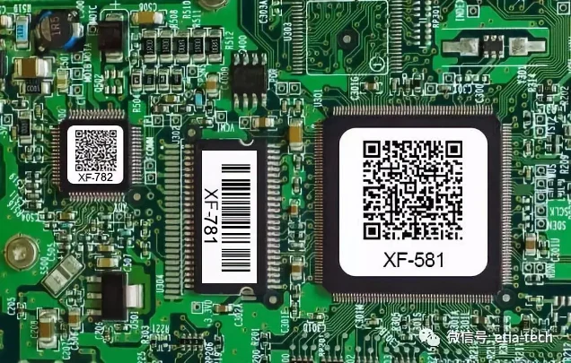
Anti-Static High-Temperature Polyimide Label
Anti-static polyimide label for ESD-sensitive electronics assembly and high-temperature…
View detailsNot sure which grade fits your printer and label?
Tell us the label material, printer model, environment and expected durability. We will recommend the right option.
